- 您现在的位置:买卖IC网 > Sheet目录3882 > PIC18F442T-E/ML (Microchip Technology)IC MCU FLASH 8KX16 EE A/D 44QFN
1997 Microchip Technology Inc.
DS30444E - page 49
PIC16C9XX
7.3.1
SWITCHING PRESCALER ASSIGNMENT
The prescaler assignment is fully under software con-
trol, i.e., it can be changed “on the y” during program
execution.
Note:
To avoid an unintended device RESET, the
following instruction sequence (shown in
Example 7-1) must be executed when
changing the prescaler assignment from
Timer0 to the WDT. This precaution must
be followed even if the WDT is disabled.
EXAMPLE 7-1:
CHANGING PRESCALER (TIMER0
→WDT)
To change prescaler from the WDT to the Timer0 mod-
ule use the precaution shown in Example 7-2.
EXAMPLE 7-2:
CHANGING PRESCALER (WDT
→TIMER0)
CLRWDT
;Clear WDT and prescaler
BSF
STATUS, RP0 ;Select Bank1
MOVLW
b'xxxx0xxx' ;Select TMR0, new prescale value and
MOVWF
OPTION_REG
;clock source
BCF
STATUS, RP0 ;Select Bank0
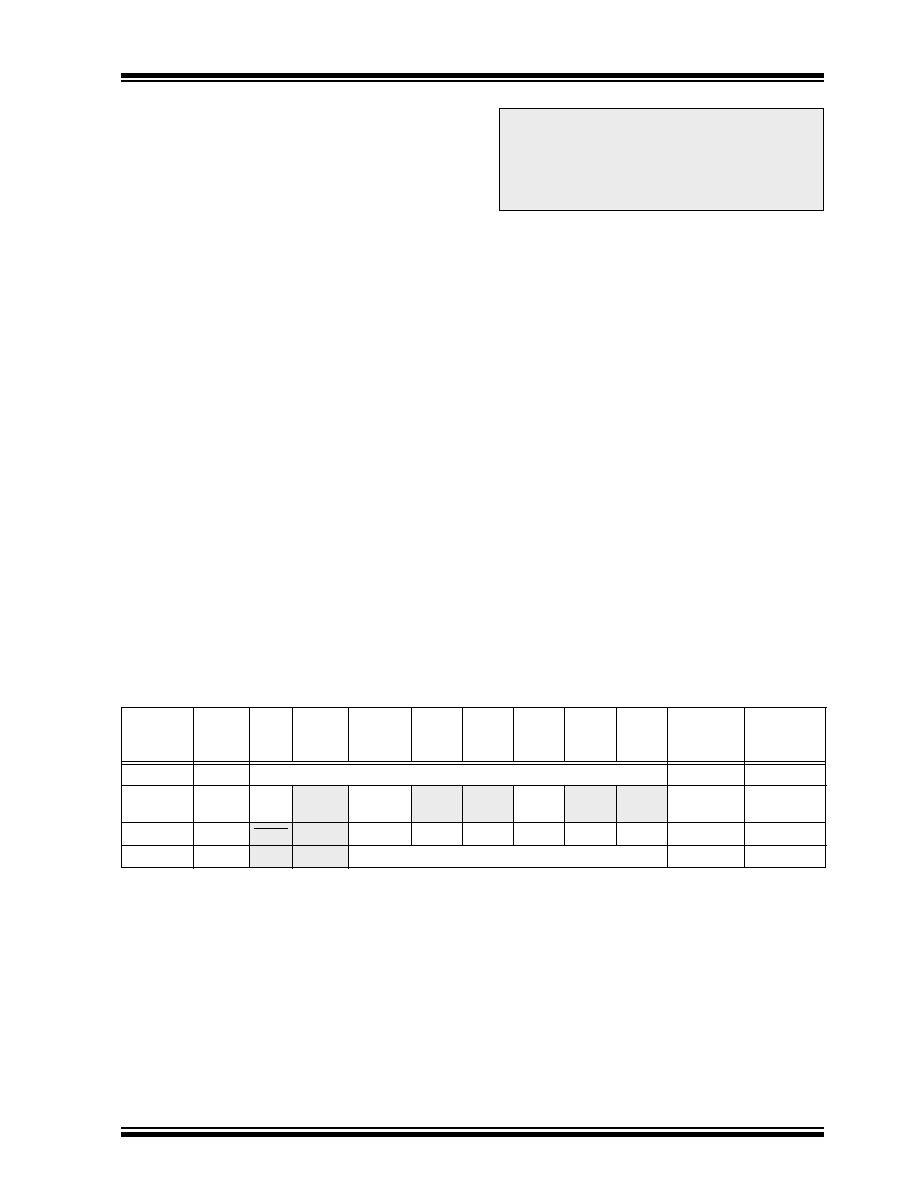
TABLE 7-1: REGISTERS ASSOCIATED WITH TIMER0
1)
BSF
STATUS, RP0
;Select Bank1
Lines 2 and 3 do NOT have to
be included if the nal desired
prescale value is other than 1:1.
If 1:1 is nal desired value, then
a temporary prescale value is
set in lines 2 and 3 and the nal
prescale value will be set in lines
10 and 11.
2)
MOVLW
b'xx0x0xxx'
;Select clock source and prescale value of
3)
MOVWF
OPTION_REG
;other than 1:1
4)
BCF
STATUS, RP0
;Select Bank0
5)
CLRF
TMR0
;Clear TMR0 and prescaler
6)
BSF
STATUS, RP1
;Select Bank1
7)
MOVLW
b'xxxx1xxx'
;Select WDT, do not change prescale value
8)
MOVWF
OPTION_REG
;
9)
CLRWDT
;Clears WDT and prescaler
10) MOVLW
b'xxxx1xxx'
;Select new prescale value and WDT
11) MOVWF
OPTION_REG
;
12) BCF
STATUS, RP0
;Select Bank0
Address
Name
Bit 7
Bit 6
Bit 5
Bit 4
Bit 3
Bit 2
Bit 1
Bit 0
Value on
Power-on
Reset
Value on all
other resets
01h, 101h
TMR0
Timer0 module’s register
xxxx xxxx
uuuu uuuu
0Bh, 8Bh,
10Bh, 18Bh
INTCON
GIE
PEIE
T0IE
INTE
RBIE
T0IF
INTF
RBIF
0000 000x
0000 000u
81h, 181h
OPTION RBPU INTEDG
T0CS
T0SE
PSA
PS2
PS1
PS0
1111 1111
85h
TRISA
—
PORTA Data Direction Control Register
--11 1111
Legend: x = unknown, u = unchanged, - = unimplemented locations read as '0'. Shaded cells are not used by Timer0.
发布紧急采购,3分钟左右您将得到回复。
相关PDF资料
PIC18LF4539T-I/ML
IC MCU FLASH 12KX16 EE A/D 44QFN
PIC18F452T-E/ML
IC MCU FLASH 16KX16 A/D 44QFN
PIC18F442-E/ML
IC MCU FLASH 8KX16 EE A/D 44QFN
PIC18F2539T-I/SO
IC MCU FLASH 12KX16 EE AD 28SOIC
PIC18F4439T-I/PT
IC MCU FLASH 6KX16 EE A/D 44TQFP
PIC16LF77T-I/ML
IC MCU FLASH 8KX14 A/D 44QFN
PIC16F74T-E/ML
IC MCU FLASH 4KX14 A/D 44QFN
PIC16F74-E/ML
IC MCU FLASH 4KX14 A/D 44QFN
相关代理商/技术参数
PIC18F442T-I/L
功能描述:8位微控制器 -MCU 16KB 768 RAM 34I/O RoHS:否 制造商:Silicon Labs 核心:8051 处理器系列:C8051F39x 数据总线宽度:8 bit 最大时钟频率:50 MHz 程序存储器大小:16 KB 数据 RAM 大小:1 KB 片上 ADC:Yes 工作电源电压:1.8 V to 3.6 V 工作温度范围:- 40 C to + 105 C 封装 / 箱体:QFN-20 安装风格:SMD/SMT
PIC18F442T-I/ML
功能描述:8位微控制器 -MCU 16KB 768 RAM 34I/O RoHS:否 制造商:Silicon Labs 核心:8051 处理器系列:C8051F39x 数据总线宽度:8 bit 最大时钟频率:50 MHz 程序存储器大小:16 KB 数据 RAM 大小:1 KB 片上 ADC:Yes 工作电源电压:1.8 V to 3.6 V 工作温度范围:- 40 C to + 105 C 封装 / 箱体:QFN-20 安装风格:SMD/SMT
PIC18F442T-I/PT
功能描述:8位微控制器 -MCU 16KB 768 RAM 34I/O RoHS:否 制造商:Silicon Labs 核心:8051 处理器系列:C8051F39x 数据总线宽度:8 bit 最大时钟频率:50 MHz 程序存储器大小:16 KB 数据 RAM 大小:1 KB 片上 ADC:Yes 工作电源电压:1.8 V to 3.6 V 工作温度范围:- 40 C to + 105 C 封装 / 箱体:QFN-20 安装风格:SMD/SMT
PIC18F4431-E/ML
功能描述:8位微控制器 -MCU 16KB 768 RAM 34 I/O RoHS:否 制造商:Silicon Labs 核心:8051 处理器系列:C8051F39x 数据总线宽度:8 bit 最大时钟频率:50 MHz 程序存储器大小:16 KB 数据 RAM 大小:1 KB 片上 ADC:Yes 工作电源电压:1.8 V to 3.6 V 工作温度范围:- 40 C to + 105 C 封装 / 箱体:QFN-20 安装风格:SMD/SMT
PIC18F4431-E/P
功能描述:8位微控制器 -MCU 16KB 768 RAM 34 I/O RoHS:否 制造商:Silicon Labs 核心:8051 处理器系列:C8051F39x 数据总线宽度:8 bit 最大时钟频率:50 MHz 程序存储器大小:16 KB 数据 RAM 大小:1 KB 片上 ADC:Yes 工作电源电压:1.8 V to 3.6 V 工作温度范围:- 40 C to + 105 C 封装 / 箱体:QFN-20 安装风格:SMD/SMT
PIC18F4431-E/P
制造商:Microchip Technology Inc 功能描述:IC 8BIT FLASH MCU 18F4431 DIP40
PIC18F4431-E/PT
功能描述:8位微控制器 -MCU 16KB 768 RAM 34 I/O RoHS:否 制造商:Silicon Labs 核心:8051 处理器系列:C8051F39x 数据总线宽度:8 bit 最大时钟频率:50 MHz 程序存储器大小:16 KB 数据 RAM 大小:1 KB 片上 ADC:Yes 工作电源电压:1.8 V to 3.6 V 工作温度范围:- 40 C to + 105 C 封装 / 箱体:QFN-20 安装风格:SMD/SMT
PIC18F4431-E/PT
制造商:Microchip Technology Inc 功能描述:IC 8BIT FLASH MCU 18F4431 TQFP44